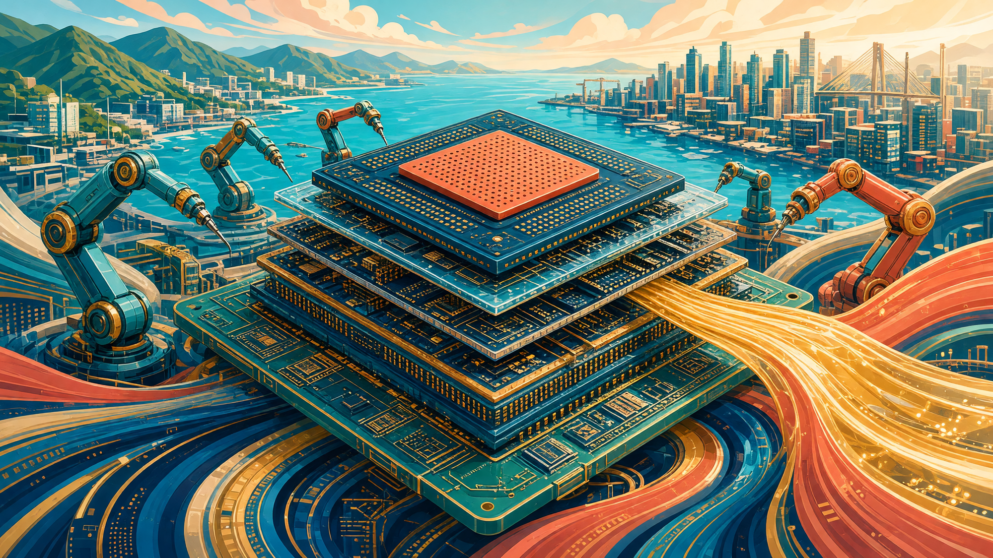
On 6 November 2026, the structural limitations of the global artificial intelligence boom came into sharp focus, revealing a critical shift in how cutting-edge hardware is manufactured. While public attention remains fixated on the raw power of new silicon designs, the semiconductor industry is increasingly constrained by an entirely different bottleneck: advanced chip packaging. In response, industry heavyweight Nvidia is now reportedly financing billions of dollars in new factories and equipment to overcome the shortage that is strictly limiting the deployment of its hardware.
This development marks a significant strategic pivot within the computing supply chain, transforming what was once a routine backend process into a fierce technological battleground. Advanced packaging refers to the intricate, highly specialised methods used to combine multiple individual semiconductors—such as logic processors and high-bandwidth memory modules—into a single, seamlessly integrated unit. As the processing demands of enterprise artificial intelligence deployments have skyrocketed, this assembly stage has become just as critical as the silicon itself.
For the Asia-Pacific region, this transition represents a profound economic opportunity and a complex logistical challenge. The region is already the historical heartland of semiconductor packaging, with deep-rooted supply chains winding through Taiwan, South Korea, and Southeast Asia. According to industry reporting on the shifting landscape, the AI boom is actively turning this packaging phase into the semiconductor market's primary arena for capital expenditure and innovation. Facilities that once managed low-margin assembly are rapidly being upgraded to handle the exacting, nanoscale precision required for high-density accelerators.
Nvidia’s unprecedented direct intervention—funnelling capital to underwrite its suppliers' physical infrastructure—underscores the severity of the bottleneck. The company is actively attempting to reshape the region’s hardware ecosystem to ensure its own product pipelines remain unclogged. By funding the expansion of these advanced facilities, the tech giant is signalling that relying on independent fabricators to scale up at their own pace is no longer a viable strategy in the current competitive climate.
For enterprise technology buyers and research institutions in Aotearoa New Zealand, the downstream effects of this packaging bottleneck are entirely practical. The cost, lead times, and availability of both cloud-based compute and on-premises AI infrastructure are now directly tethered to the production capacity of these APAC-based packaging plants. While Aotearoa operates at the edge of this physical supply chain, our domestic tech sector relies heavily on the uninterrupted flow of these tightly integrated systems.
The era of relying solely on shrinking transistors to drive exponential computing gains is fading. As the foundational architecture of artificial intelligence scales up, the physical realities of hardware assembly are enforcing new limitations. The battle for AI infrastructure supremacy is no longer just about designing the smartest chip; it is now equally about mastering the complex engineering required to wire them together.
Sources
- Yahoo Finance; Nvidia Is Reportedly Pouring Billions Into AI's Next Big Bottleneck
- The HinduBusinessLine; AI boom turns advanced chip packaging into the next battleground
AI disclosure: Automated systems assisted with research and drafting. Gemini independently peer-reviewed this article before publication. Sources are linked for verification.